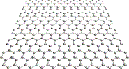
Graphene
In 1962, Hanns-Peter Boehm described single-layer carbon foils and coined the term "graphene", graphite with the "ene" suffix.
In 2004, Andre Geim, Kostya Novoselov and co-workers at the University of Manchester produced a sheet of graphene and studied its properties.1
Graphene was the first truly 2-dimensional crystal ever observed in nature, and, because graphene is harder than diamond, tougher than steel, light weight, transparent, flexible and extremely conductive, graphene is regarded as the material of the future.
It could make computers faster, mobile phones more flexible, and touch-screens thinner.
Carbon, Group 14 of the periodic table, has 4 valence electrons as shown in the Lewis Structure below:
Each carbon atom is capable of forming 4 covalent bonds, but, in graphene, only 3 covalent bonds are formed:
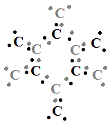
In the Lewis Structure shown above, electrons that appear on their own will actually be paired with another electron from another cabon atom in order to form an infinite lattice of carbon atoms held together by covalent bonds:
The angle between the carbon atoms (the C-C-C bond angle) is 120°, making a perfectly symmetrical hexagonal lattice of carbon atoms
that looks a lot like chickenwire or honeycomb and contains 3.9 × 10¹⁵ carbon atoms in each cm2 of graphene, resulting in a low density material.
The bonds between carbon atoms are all covalent bonds, making the 2-dimensional lattice strong, that is, it requires a great deal of energy to break the C-C covalent bonds.
Indeed, graphene is one of the strongest materials known, yet it has a low density.
The Nobel Prize announcement illustrated this as:
1 m2 of graphene hammock would support a 4 kg cat but would weigh only as much as the cat's whiskers, about 0.77 mg
So, if three of each carbon atom's electrons are directly involved in the formation of covalent bonds with a neighboring carbon atom, what happens to the fourth valence electron on each carbon atom?
This electron is said to be delocalised.
The half-filled orbitals of the carbon atoms make up a band which permits free-moving electrons.
This is reflected in the length of the bonds between carbon atoms which are about 1.42 Å (0.142 nm) in graphene, that is, between the C-C single bond length of 0.154 nm and the C=C double bond length of 0.134 nm.
Because of this, graphene displays remarkable electron mobility at room temperature, about a million times better than copper which is commonly used in electrical wiring.
Graphene is therefore an excellent conductor of heat and electricity because the interactions between electrons and graphene's honeycomb lattice causes the electrons to behave as if they have absolutely no mass.
Because of this, the electrons in graphene show relativistic behaviour at speeds much slower than the speed of light, that is, at 106 ms-1 rather than 3 × 10⁸ ms-1.
Graphene could be used as a bench-top particle physics laboratory, allowing physicists to investigate the quantum field theories that describe the fundamental interactions of matter without the need for huge particle accelerators.
Metals are also good conductors of heat and electricity but impurities in the metal crystal scatter electrons leading to energy loss.
In graphene, the electrical resistance is independent of the number of impurities.
This means that electrons can travel for many micrometres through graphene without colliding with any impurities, making graphene a promising material for a potential high-speed electronic switching device callled a "ballistic transistor".
Graphene-based electronics could improve the current level of miniaturisation by an order of magnitude.
Graphene's conduction can be made to depend on an ambient electric field, making it a very sensitive surface.
Metal films cannot be made as thin so they are less sensitive than graphene.
So graphene could be used to detect single molecules of a gas.
If a gas molecule were to stick to a sheet of graphene there would be a local change in the electrical resistance.
This could also be useful for detecting microbes.
For the same reason, graphene could be used as a touch screen surface.
In 2015 researchers used graphene to create sensitive biosensors which could be used to predict a person's risk of developing several cancers.
Graphene could potentially replace the tungsten and silicon electrodes used in medicine because it is flexible, conductive, and is not known to be harmful.
Graphene can self-repair holes in its sheets when exposed to molecules containing carbon such as hydrocarbons.
Bombarded with pure carbon atoms, the atoms perfectly align into hexagons, completely filling any holes.
The surface area of a sheet of graphene compared to a bulk material like coal is enormous.
The surface area of graphene is 2630 m2 g-1, larger than that reported for bulk carbon which is about 900 m2 g-1.
Therefore, we expect graphene to be more chemically reactive than bulk carbon materials.
But the chemical reactivity of graphene is also increased because graphene has a 2-dimensional structure, every carbon atom is available for chemical reaction from two sides.
Graphene has the highest ratio of edge atoms of any allotrope of carbon and these atoms at the edge of a graphene sheet have special chemical reactivity because they have made only 2 covalent bonds, therefore they have 2 unpaired (non-bonding) electrons.
Likewise, defects within a sheet can also increase its chemical reactivity.
In 2013, Stanford University physicists reported that single-layer graphene is a hundred times more chemically reactive than thicker sheets.
For example, a sheet of graphene burns at very low temperature, 350°C.
Even so, graphene is still relatively chemically inert because the "large scale" delocalisation of electrons also makes graphene more chemically stable than expected.
Graphene is highly resistant to attacks by strong acids or strong alkalis and so can be used to give surfaces an ultra-thin protective layer which is transparent.
Graphene is strong, thin, and transparent, so it can be used as a support membrane for transmission electron microscopy because it does not interfere with the image generated by the electron microscope.
Transmission electron microscopy is used to study the molecular detail of materials such as fragile DNA molecules and nanoparticles themselves.
By creating nanoscale pores in a sheet of graphene, graphene membranes can be used as a highly selective filter material.
This could lead to more efficient methods for the desalination of seawater.
Water molecules could diffuse through the graphene membrane, leaving behind the larger hydrated ions from the salts found in seawater.
Researchers in China have discovered that graphene has some antibacterial properties and is effective at killing E Coli bacteria, leading to suggestions for its use in hygiene products.
In 2016, Brown University introduced a method for "crumpling" graphene, adding wrinkles to the material on a nanoscale.
This was achieved by depositing layers of graphene oxide onto a shrink film.
The film was then shrunk, then the film was dissolved, then the graphene sheet shrunk again on another sheet of film.
The crumpled graphene became superhydrophobic (water hating), and, when used as a battery electrode, the material was shown to have as much as a 400% increase in electrochemical current density.
Production of Graphene
There are three methods for producing graphene:
- mechanical exfoliation of graphene from bulk graphite
- graphitisation of epitaxially grown silicon carbide crystals
- substrate-free synthesis
The mechanical exfoliation technique consists of peeling off layers from graphite.
Whenever you write with a "lead" pencil (actually a graphite pencil) thin graphite stacks are exfoliated from the bulk material and are left behind on the substrate (paper for instance).
Most of these thin stacks are made up of several, even tens or hundreds, of graphene sheets, but a few of them will consist of only one single graphene layer.
In practice, scientists prepare very thin samples by peeling a small graphite crystallite in a piece of folded stickytape (scotch tape).
Each time the tape is peeled away, the graphite flake is cleaved in two parts and thus becomes thinner.
After several cycles the tape with the graphene sheet stuck to it is glued to a silica substrate.
When the tape is carefully peeled away, the graphene sheets remain glued to the silica substrate.2
An alternative technique for producing graphene has been developed by the Atlanta Group led by Walt de Heer and Claire Berger.
This consists of exposing an epitaxially grown hexagonal silicon carbide (SiC) crystal to temperatures of about 1300°C in an argon atmosphere in order to evaporate the less tightly bound silicon atoms from the surface.
The remaining carbon atoms on the surface form a graphitic layer (graphitisation).
The technique produces layers of graphene, one on top of the other, but they are further enough away from each other to act as independent units (unlike the bound layers in bulk graphite).
The layer closest to the substrate surface is electron-doped due to a charge transfer from the bulk SiC, whereas the subsequent layers are hardly charged at all.
Interaction with the substrate limits the mobility of the electrons so hydrogen is introduced into the interface between the two materials (a method known as hydrogen intercalation).
The bonds between the graphene and the substrate material are separated and saturated by the hydrogen atoms.
This suppresses the electronic influence of the silicon crystal while the graphene stays mechanically joined with the substrate.
For practical applications, the electrical properties of graphene must be modifiable, for example by introducing additional electrons into the material.
This is effected by targeted "contamination" of the carbon lattice with foreign atoms.
For this process, known as "doping", the graphene is bombarded with nitrogen ions and then annealed (a process of heating and cooling in order to toughen the material).
This results in defects in the lattice structure: some carbon atoms, fewer than 1%, separate from the lattice and are replaced with nitrogen atoms, which bring along additional electrons.
Graphene doped with various gases can be returned to an undoped state by gently heating in a vacuum.
The graphitisation of epitaxially grown SiC crystals could form the basis of commercial-scale production of graphene.
The search for a suitable substrate material on which to grow graphene is one of the major challenges on the path towards practical applications because if undesirable interactions occur they can cause graphene to lose its electric properties.
The "Tau-Lau Method" for producing graphene is effectively a substrate-free technique using a sugar like glucose.
It is a bottom-up synthesis which can control thickness from monolayer to multilayers.
Buckminsterfullerene
In 1985, Robert Curl, Harold Kroto, and Richard Smalley discovered the graphitic allotropes known as fullerenes.3
The most prominent member of this group is the C60 molecule, called Buckminsterfullerene4, also known as a "buckyball", which is made up of 60 carbon atoms as shown below:
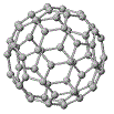
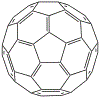
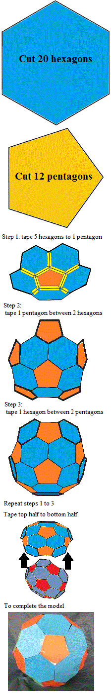
Buckminsterfullerene (buckyball) has the form of a soccer ball (football) that is, a truncated icosahedron made up of 20 hexagons and 12 pentagons (follow the instructions on the right to make a model of a buckyball).
There is 1 carbon atom at each vertex in the model of C60 on the right, and is roughly spherical in shape with a diameter of about 1 nm.
Buckminsterfullerene's structure consists of localised single bonds, C-C, between hexagons and pentagons and double bonds, C=C, between two hexagons, as shown in the skeletal structure below:
Unlike graphene, there are no delocalised electrons in the C60 (buckyball) structure.
Buckminsterfullerene can undergo addition reactions because it contains double bonds, C=C.
Hydrogen can "add" across the double bonds in a hydrogenation reaction quite easily.
One fullerene molecule can hold up to 36 hydrogen atoms.
The colour of hydrogenated fullerenes changes from black to brown, red, orange and finally yellow as the hydrogen content increases:
| low hydrogen content |
→ → → → |
high hydrogen content |
| |
|
|
|
|
Currently, compressed hydrogen gas or metal hydrides are used as hydrogen storage technologies but these are potentially hazardous and/or have low hydrogen storage densities.
Fullerene hydrides offer a better, safer, more efficient hydrogen storage option for uses such as fuel cells in electric vehicles.
The reactivity of the double bonds enables the C60 molecule to be modified in other ways so that it can be used in a range of applications.
For example, fullerenes are not soluble in water, and have a tendency to form aggregates.
By surrounding (encapsulating) the hydrophobic (water hating) fullerene with hydrophilic (water loving) molecules, fullerenes can be suspended in aqueous solutions.
This is useful in biological applications.
For example, derivatives of fullerenes are being used for drug delivery, the transportation of a pharmaceutical compound to its site of action.
Being so small, fullerene can easily diffuse through the skin intact so a hydrophobic (water hating) drug could be delivered via the skin into the system.
Amino acid derivatives of fullerenes are being investigated for their antiviral antibacterial properties.
Suitable non-toxic fullerene derivatives can be used in Photodynamic Therapy which is used to target altered and malignant cells.
Fullerenes get excited upon irradiation, when these molecules return to the ground state, they give off energy that splits the oxygen present to generate singlet oxygen which can be toxic to cells.
Fullerenes make excellent antioxidants.
They can react with a number of radicals, highly reactive species with a lone electron, before being used up, and are sometimes referred to as "radical scavengers" or "radical sponges".
A "radical sponge" is often added to cosmetics to prevent skin damage and premature aging of the skin because they also protect against ultraviolet radiation.
Because fullerenes have a high electron affinity and are able to transfer electrons in excited states, it is hoped that organic photovoltaic cells can be produced which will be complexes of fullerenes and polymers.
The cost of production of solar cells using fullerenes would be lower than that of conventional solar cells, and, these organic solar cells would be very flexible so they could be rolled up, cut, and spread over any surface.
Imagine coating a mobile phone (cell phone) with this material, just walking in the sun would be enough to recharge the battery!
Other uses would be to create luminous banners and displays.
The high electron affinity of fullerenes could also be used to produce molecular wires which will be needed if a molecular computer is to be built in the future.
|
Build a model of a buckyball:
|
Buckminsterfullerene can be doped with alkali metal atoms, that is, alkali metal atoms can fit between the buckminsterfullerene molecules making up the solid material.
Potassium-doped buckyballs become superconductors at 18 K (-255°C), that is, an electrical current can flow without resistance.
Under pressure, caesium-doped fullerene becomes a superconductor at 38 K (-235°C).
Fullerenes have the ability to decrease the transmittance of incident light (called optical limiting), so they could be used to produce protective eye wear.
Buckminsterfullerene has a high melting and boiling point and a very high tensile strength so that the molecules will bounce back to their original shape after being subjected to high pressures.
It is hoped that fullerenes can be dispersed through a metal matrix so that lightweight ductile metals with greater tensile strength can be developed.
Fullerenes can be used to produce diamonds which grow at 5 times the rate of diamonds produced using methane carbon sources.
This results in a massive cost savings for the commercial production of diamonds.
The 60 carbon atoms making up buckminsterfulleren effectively form a cage and it is possible to insert other atoms into this cage.
When a metal atom is inserted into the cage we refer to the molecule as a metalofullerene, gadofullerene for example is formed when gadolinium atoms are inserted into the cage.
Metalofullerenes are used as contrast agents in X-ray and MRI imaging.
Carbon Nanotubes
Soviet scientists Radushkevich and Lukyanovich published a transmission electron microscope image showing carbon nanotubes in 1952 but it aroused little scientific interest.
It wasn't until the publication of a paper in 1991 by Sumio Iijima that scientific interest became intense.
Carbon nanotubes are also known as fullerene tubes or buckytubes and can be thought of as graphene sheets which are rolled up, as shown in the diagram below:
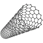
The diameter of a carbon nanotube is tiny, up to a few nanometres wide, but they can be very long.
Note that every carbon atom (except those at the edges) is covalently bonded to 3 other carbon atoms, which makes carbon nanotubes very strong, about twice as strong as steel.
But carbon nanotubes weigh about 6 times less than steel because they have a low density, even lower density than aluminium (which is a low density metal).
Because of their low density, objects made out of carbon nanotubes don't weigh much so they can be used to make strong ropes that are lighter than the strongest ropes we have today.
Some scientists are even working on a "space elevator" that will use a carbon nanotube rope to take us all the way into space!
Carbon nanotube fibers can be used in composite materials to produce reinforced, light-weight materials used in sporting goods such as bicycles, tennis rackets and golf clubs.
Specific surface area of carbon nanotubes is of the order of 100 - 1000 m2 g-1, less than for graphene, but still huge.
This enormous surface area means that carbon nanotubes could be used to produce better catalysts.
The catalyst can be attached to the carbon nanotubes increasing the available surface area of the catalyst.
This will inrease the rate of the chemical reaction, making an industrial process more efficient and more economic.
You can heat up carbon nanotubes up to 750°C and they won't melt or burn and they even conduct heat and electricity better than most other materials.
When a carbon nanotube is put into an electric field, it will emit electrons from the end of the nanotube like a small cannon.
If these electrons are allowed to bombard a phosphor screen then an image can be created.
In the spring of 2005, Motorola announced a new "NanEmissive Display" (NED) technology, making more energy efficient and cost-effective ultra-flat display screens a reality.
The behaviour of electrons depends on the length of the carbon nanotube, so some forms are excellent conductors and others are semiconductors.
Semiconducting carbon nanotubes display a large change in conductance, that is in the ability to store charge, in the presence of gases such as nitrogen dioxide (NO2(g)) and ammonia (NH3(g)).
By exposing carbon nanotubes to a gas and then measuring the change in conductance, they can be used as sensors.
Carbon nanotube sensors are smaller, more sensitive, and respond faster than conventional sensors.
In 2005, Naval Research Laboratory scientists used a prototype nanotube gas sensor to detect minute amounts of sarin gas in under 4 seconds using a prototype nanotube gas sensor. Conventional gas sensors available at that time took over a minute to detect the same amount.
Scientists have been able to use semiconducting nanotubes as compact, more efficient alternatives to transistors, devices used in electronic equipment that can act like an on/off switch or an amplifier for current.
Carbon nanotubes could revolutionise electronics because of their nanoscale dimensions and very low electrical resistance but there have been problems producing nanotubes with well-defined sizes.
There is another problem using nanotubes in electrical circuits because the metal contacts that connect them to circuits have a higher resistance than the nanotubes, which produces a lot of heat during operation, so it is difficult to integrate nanotubes into electronic devices on a mass-production scale.